

Contract Processing
1
High Accuracy, High Quality and Acceptance of Small Lots
We have an esteemed reputation for achieving ultimate preciseness of submicron orders and surface smoothness at an atom-level.
2
Capable of Preparing Material (if requested)
We can arrange material such as glass and sapphire before processing, as well as processing supplied material.
3
We put full effort on Processing Resistant Material
We will try our best on materials which have been turned down by other companies, as our strengths as a company is having several methods of processing.
- Capability of achieving high-quality, high flatness on both sides of the board
- Prototype processing (1 piece~) ~ medium size in lots (~ x000/month) *depends on material
- From procurement of material, we will take care of every single step of your product
- Capability of processing material thinner than 100μm
- Capability of processing a variety of materials (e.g. Advanced crystal material, metals, rubber etc.)
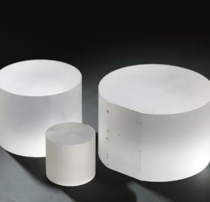
PROCESSING TECHNOLOGY
| Cutting | We are capable of precisely cutting material by multi-wire/single-wire saws, and also process cutting glass material. Max. cutting ingot size is, 150mm in diameter x 150mm in length |
|---|---|
| Grinding | We are capable of precisely applying the final touch for squint basal plates (diameter; few mm~ 100mm) |
| Heat Treating | We can apply heat treating for removing processing-distortions(~1800℃) |
| Polishing | We will utilize the most ideal polishing method out of a variety of procedures such as lapping, machine polishing (MP), chemical machine polishing (CMP) and so on. Whether it’s single sided or double sided, we can meet your expectations. |
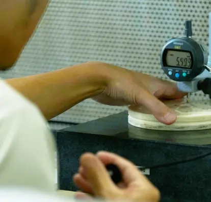
| Measurement Evaluation | We can assess the quality of shape and surface of the material. (max diameter=150mm) Shape evaluation
|
PRODUCT MACHINING RESULT
| Single crystals | Sapphire,SiC,GaN,Diamond,Si,Quartz,AlN,LiTaO3, LiNbO3,MgF2,CaF2,Ga2O3 |
|---|---|
| Polycrystalline and ceramics | Al2O2、AlN、SiN、Zr O2、SiC、Diamond、Glass ceramics |
| Metals | SUS,Al,Cu,Ni,Cemented carbide,Ti,Inver |
| Resin | PC,PMMA, Epoxy,PVC,CFRP |
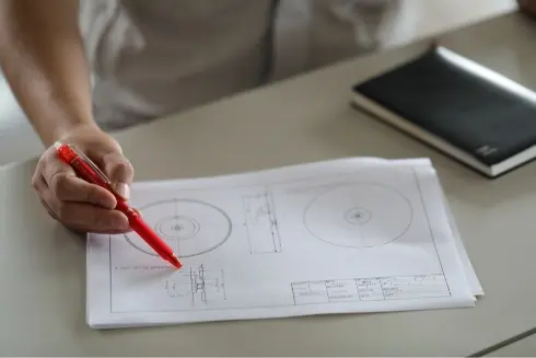
PROCESSING REQUEST
1
Please contact us through “inquiries”.
If you have requests regarding material, shape, quantity, accuracy or delivery schedules, please don’t forget to let us know. If you wish, we can arrange a meeting on/offline to discuss details.
2
Based on the type of material, one of our departments will reach you for confirmation.
3
Submission of official quotation
4
Manufacture process
5
Delivery